

Semiconductor materials and photonics
Research is focused on the epitaxial growth of new semiconductor materials and the investigation of the underlying physics which determine the efficiency limiting processes in infrared light sources, thermo-photovoltaics and solar cells.
Key research areas
- Mid-infrared LEDs and laser for gas sensing and environmental monitoring
- Thermophotovoltaic cells for industrial waste heat recovery
- Infrared photodetectors for thermal imaging
- Quantum dot lasers for telecommunications
- Solar cells for renewable energy generation.
Research themes
Solar cells
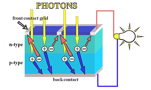
The Intermediate Band Solar Cell (IBSC) is a concept that has the potential to increase the efficiency to 63%. The intermediate band acts as a ‘stepping stone’ allowing absorption of photons (energy particles from the sun) from three distinct levels compared to a single level in conventional SCs. We are developing nanostructured IBSCs using GaSb Quantum Rings.
Mid-infrared photonics
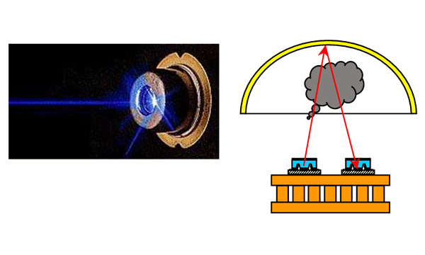
III-V semiconductors based on the family of 6.1 Ȧ semiconductors which includes InAs, GaSb, AlSb and related alloys have a wide range of band gaps that corresponds to the mid-infrared spectral range (MIR) (2-5 µm), where many molecules such as hydrocarbons and greenhouse gases have their absorption lines.
Key information
People
Facilities
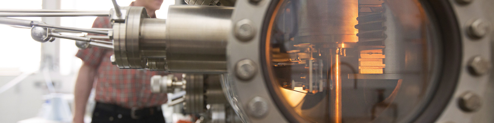
- Veeco Xplor System
Ultra-high vacuum system designed to grow a wide range of III-V materials. The system is designed with a specially designed substrate heater for III-V/Silicon integration. - Quantum Technology Centre
Our devices are processed in the state-of-the-art QTC clean room.